
Aluminum has transcended from being a trend in the furniture business to becoming an essential part of most brands’ collections.
In the outdoor furniture business, Aluminum collections have proven their superiority in many aspects.
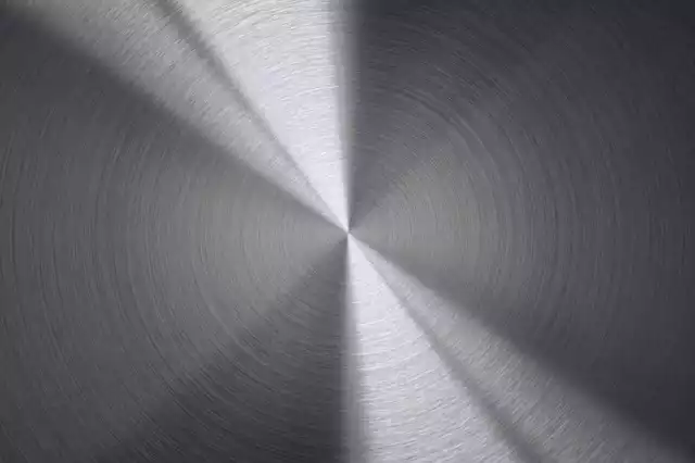
Aluminum is strong, light and resistant to corrosion.
It comes in tubular form and cast form.
Aluminum was discovered in 1821 but was not available in industrial quantities until years later.
Its uses now are endless but we notice it mostly in furniture, electronics and high end gadgets.
Imagine a world where your smartphone disintegrates in your pocket, or your smartwatch shatters at the slightest bump.
These nightmare scenarios highlight the hidden heroes of modern technology: materials. The unseen skeletons and skins of our gadgets are engineered with such precision and innovation that they withstand daily wear and tear, all while delivering seamless performance.
In this article, we’ll peel back the sleek exteriors of your favorite tech devices to uncover the fascinating science behind Materials for Gadgets and their construction.
From ultra-durable glass to flexible polymers and cutting-edge metals like titanium and graphene, the materials that make gadgets are as crucial as their software counterparts.
Join us on an exploration into these marvels of modern engineering—materials that do more than just hold our devices together; they redefine what’s possible in the world of technology.
Table of Contents Materials for Gadgets
STRENGTH AND LONGEVITY

The most commonly thought of things that make aluminum the perfect material as a choice for outdoor furniture are its longevity and strength.
Whether you live in areas where the summers are harsh or in a place with soaking wet tropical weather, aluminum is the material for you! Unlike wooden furniture, water has zero effect on aluminum.
Direct scorching sun does not affect aluminum itself, but merely hits the finishing or paint only.
LIGHT-WEIGHT
The distinctive aspect of this metal is that it is very light compared to what it offers in strength and robustness! Before being used in furniture, aluminum was used in motorsports and aerospace engineering due to these attributes.
Everyone rearranges outdoor furniture numerous times a year, whether for cleaning purposes, seating arrangements or even just for general ambiance, patio furniture needs to be light in order to be malleable.
Aluminum furniture is easy to move and can give you the freedom to redesign whenever you feel like it.
RUST-FREE
Although metal furniture is old on the market, aluminum specifically made a boom in the past years for one major reason, NO RUST!
The scientific explanation to this is that on its surface, Aluminum binds itself to airborne oxygen and forms a thin layer of Oxide.
This turns it completely corrosion resistant.
This makes your garden furniture safe when exposed to most conditions thrown at it.
Other than a light wiping every now and then to remove stains, your furniture stays self-sufficient for years to come!
VARIETY
Aluminum handling has moved to become one of the most malleable furniture frame materials ever.
Bending, twisting and welding aluminum has moved to new heights.
Combine that with the many colors you can paint it with and you find yourself with endless possibilities.
POWDER COATING
Powder coating is the preferred way to paint aluminum as it binds better than regular paint.
In recent years, most manufacturers powder coat aluminum electrostatic-ally.
This is when they charge the paint/spray gun with a charge opposing what they charged the piece of furniture with.
The opposing charges cause the paint to adhere to the aluminum uniformly and with very little residue or waste! The piece is then heated in order to make the paint form a sort of skin that is very hardly affected by scratches and bumps.
Materials used to make Semiconductor Wafers
Typically, wafers are made using pure silicon grown into monocrystalline cylindrical ingots (boules) up to 300 into in diameter.
That is when you use the Czochralski process.
A point to note is that wafers are usually in rods that are in specific diameters.
The silicon used for making wafers is often derived from sand.
Some of the attributes if silicon that make it ideal for this job is that is readily available and environmentally friendly as well.
Manufacturing Process of Semiconductor Wafers
The Process
The steps in semiconductor wafer manufacturing are divided into four categories namely deposition, removal, patterning as well as modification.
Deposition
This is the process of growing, coating or transferring materials onto a wafer.
The available technologies for this include electrochemical deposition ([CD), chemical vapor deposition (CVD), physical vapor deposition (PVD), atomic layer deposition (ALD) molecular beam epitaxy (MBE).
emoval
This is the process of removing materials from the silicon wafer, and this includes etch processes which may be dry or wet as well as the chemical-mechanical planarization (CMP).
Patterning
This entails the altering or shaping of the deposited materials and is normally referred to as lithography.
In traditional lithography, a chemical called photoresist is used for coating the wafer and a machine known as a stepper is used to focus, align and move a mask.
This helps to expose some parts of the wafers to short wavelength light.
The exposed parts are simply washed away using a developer solution.
A plasma ashing will be used to remove any remaining photoresist after the process of etching or any other similar process.
Modification
Historically, the process of modifying electrical properties involved doping transistor drains and sources (originally through diffusion furnaces and ion implantation).
Furnace annealing comes after these doping processes.
If the device is advanced, the rapid thermal annealing will follow the doping processes (RTA).
Annealing activates the dopants which are implanted.
Modifying electrical properties also extends to reducing the dielectric constant in materials found in low-k insulators through the introduction of ultraviolet light in UV processing (UVP).
Modern chips have about eleven levels of metals that are produced in more than 300 processing steps that are sequenced.
Building foundation for Wafers (Wafers)
After extracting silicon from the sand, it undergoes a purification process that entails heating it until it becomes a high-purity liquid.
It then solidifies into an ingot through methods such as the Floating zone process or Czochralski (chokh-RAL-skee).
The latter method makes use of a tiny piece of well done solid silicon that is put in polycrystalline or molten silicon and brought in a rotation.
This is done as the liquid becomes a cylindrical ingot.
This is the reason why the complete wafers have round disc shapes.
Wafer Thin
Before it completely cools down, the ends of the ingot which are cone-shaped are then cut off as the body of the silicon is cut into gaunt wafers.
At this point, the wafers have a uniform thickness and entail diamond sharp saw blades.
This is the reason why the diameter of the ingot determines the wafers size.
Previously, the manufacturers had only three-inch diameters.
Things have since changed as diameters are increasing in size because there are now larger wafers.
People who have larger wafers enjoy higher productivity and more chips.
At the moment, the biggest diameter in the semiconductor industry is 300mm or 12 inches.
Polishing and Lapping
You should prep sliced wafers first to ensure they are production-ready.
One way of doing this is to polish them, and you can do this using abrasive machines and chemicals on the uneven surfaces for a mirror —smooth finish.
A flawless surface will allow circuit patterns to form well on the surface of the wafer during the process of lithography.
Parts of a Semiconductor Wafer
Chip
This entails a small silicon piece with some electronic patterns.
Scribe Lines
These are non-functional, thin spaces found between functional pieces that allow a saw to safely cut your wafer without having to damage the circuits.
TEG
(Test Element Group) is an elaborate prototype that shows the real chip characteristics (transistors, circuits, capacitors, diodes and resistors) to make it easier to know if they were working as expected.
Edge Die
The chips (dies) found at the wafer edge is commonly seen as a production loss.
Normally, larger wafers would have fairly less loss of chips.
Flat Zone
The flat zone at the end of the wafer is cut off and that is to aid in identifying the type and orientation of the wafer.
The flawless surface of the wafer ensures the successful formation of circuit patterns during lithography.
A small silicon piece with electronic patterns is involved in this process. Scribe lines, non-functional spaces, are strategically placed between functional pieces to allow safe cutting of the wafer without damaging the circuits.
TEG, or Test Element Group, is a detailed prototype that helps assess the performance of various chip characteristics such as transistors, circuits, capacitors, diodes, and resistors.
Edge die, often seen as a production loss, refers to the chips located at the wafer’s edge, with larger wafers typically experiencing lower chip loss.
The flat zone at the end of the wafer is removed to aid in identifying the wafer’s type and orientation.